- 您现在的位置:买卖IC网 > Sheet目录1223 > KIT34674EPEVBE (Freescale Semiconductor)KIT EVAL BOARD 10CH LED BACKLGHT
�� �
�
�FUNCTIONAL� DESCRIPTION�
�FUNCTIONAL� INTERNAL� BLOCK� DESCRIPTION�
�FUNCTIONAL� INTERNAL� BLOCK� DESCRIPTION�
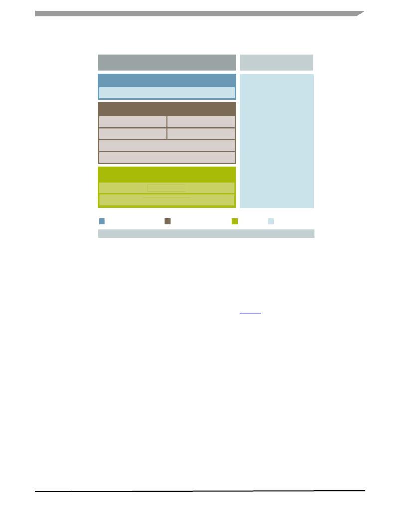
�MC34674� -� Functional� Block� Diagram�
�Integrated� Supply�
�Internal� Supply� &� Reference�
�Sensing� &� Control�
�VIN� Monitor�
�End of Charge�
�Charge Control�
�VIN - BAT Compare�
�Die Temperature Feedback�
�NTC� Thermistor� Interface�
�Logic�
�Logic Contro� l�
�Status� Indication�
�Power� MOSFET�
�Integrated� Supply�
�Sensing� &� Control�
�Logic�
�MOSFET�
�Figure� 18.� 34674� Functional� Internal� Block� Diagram�
�INTEGRATED� SUPPLY�
�conditions� are� reached,� this� block� outputs� a� logic� signal� to�
�indicate� the� end� of� the� charge.�
�INTERNAL� SUPPLY� AND� REFERENCE�
�The� internal� supply� and� reference� block� steps� down� the�
�high� input� voltage� to� a� lower� voltage� to� power� all� the� internal�
�control� blocks.� In� addition,� this� block� generates� the� reference�
�voltages� for� other� functional� blocks.�
�SENSING� AND� CONTROL�
�VIN� MONITOR�
�The� VIN� monitor� block� monitors� the� input� voltage� for� two�
�thresholds,� power-on-reset� (POR)� and� over-voltage�
�protection� (OVP).� If� the� input� is� lower� than� the� POR� or� higher�
�than� the� OVP� threshold,� this� block� outputs� a� logic� signal� to�
�disable� the� charger.�
�CHARGE� CONTROL�
�The� charge-control� block� controls� the� gate� voltage� of� the�
�power� MOSFET� to� regulate� the� charge� current,� the� battery�
�voltage,� or� the� die� temperature.� It� can� also� completely� turn� off�
�the� power� MOSFET� to� stop� the� current� flow� between� the�
�input� and� the� battery.�
�EOC� (END� OF� CHARGE)�
�The� EOC� block� monitors� the� charge� current� and� the�
�VIN-BAT� COMPARATOR�
�The� VIN-BAT� comparator� monitors� the� voltage� difference�
�between� the� input� voltage� V� IN� and� the� battery� voltage� V� BAT� ,�
�as� shown� in� Figure 2� .� The� input� voltage� has� to� be� higher� than�
�the� battery� voltage� for� the� charger� to� be� enabled.� If� the� input�
�voltage� falls� below� the� battery� voltage,� this� block� outputs� a�
�signal� to� disable� the� charger� to� prevent� the� leakage� current�
�from� the� battery� to� the� input.� Due� to� the� intrinsic� input� offset�
�voltage� of� the� VIN-BAT� comparator,� a� small� voltage,� V� OS� ,� is�
�added.� The� added� V� OS� guarantees� that� the� power� MOSFET�
�is� turned� off� when� the� input� voltage� is� lower� than� the� battery�
�voltage.�
�DIE� TEMPERATURE� FEEDBACK�
�The� die� temperature� feedback� block� monitors� the� die�
�temperature.� Once� the� die� temperature� reaches� a� threshold�
�of� 110°C,� the� charge-control� block� can� reduce� the� charge�
�current� to� prevent� further� temperature� rise.�
�NTC� INTERFACE�
�The� NTC� interface� block� offers� an� interface� to� an� external�
�NTC� thermistor� circuit� to� monitor� the� battery� temperature� and�
�to� set� the� charge� temperature� window.�
�battery� voltage� for� the� EOC� conditions.� Once� the� EOC�
�34674�
�Analog� Integrated� Circuit� Device� Data�
�Freescale� Semiconductor�
�13�
�发布紧急采购,3分钟左右您将得到回复。
相关PDF资料
KIT34675EPEVBE
KIT EVALUATION FOR MC34675
KIT35XS3500EVBE
KIT EVAL QUAD HIGH SIDE SWITCH
KITUSBSPIEVME
KIT EVAL USB-SPI W/MC68HC908JW32
KP3040
KEYPAD USB W/2 USB PORTS
KS8737-EVAL
BOARD EVAL EXPERIMENT FOR KS8737
KSZ8695PX-EVAL
KIT EVAL KSZ8695PX EXPERIMENT
KSZ9692PB-EVAL
BOARD EVALUATION FOR KSZ9692PB
L17-RR-D1-F-01-100
CONN SOCKET 20-24AWG CRIMP GOLD
相关代理商/技术参数
KIT34675EPEVBE
功能描述:电源管理IC开发工具 28V-INPUT-VOLT SNGL RoHS:否 制造商:Maxim Integrated 产品:Evaluation Kits 类型:Battery Management 工具用于评估:MAX17710GB 输入电压: 输出电压:1.8 V
KIT34676EPEVBE
功能描述:电源管理IC开发工具 DUAL 28V-INPUTVOLT C RoHS:否 制造商:Maxim Integrated 产品:Evaluation Kits 类型:Battery Management 工具用于评估:MAX17710GB 输入电压: 输出电压:1.8 V
KIT34676EPEVBE
制造商:Freescale Semiconductor 功能描述:Dual 28V input voltage single cell Li-Io
KIT3468MMA7455L
功能描述:加速传感器开发工具 3-AXIS 2G ,4G, 8G Dig Out, Dev Kit RoHS:否 制造商:Murata 工具用于评估:SCA3100-D04 加速:2 g 传感轴:Triple Axis 接口类型:SPI 工作电压:3.3 V
KIT3468MMA7455L
制造商:Freescale Semiconductor 功能描述:Output Accelerometer Evaluation Board
KIT3468MMA7456L
功能描述:加速传感器开发工具 XYZ-AXIS DIGITAL 2G4G RoHS:否 制造商:Murata 工具用于评估:SCA3100-D04 加速:2 g 传感轴:Triple Axis 接口类型:SPI 工作电压:3.3 V
KIT34700EPEVBE
功能描述:电源管理IC开发工具 4 Output Integrated Pwr Supply Eval Kit RoHS:否 制造商:Maxim Integrated 产品:Evaluation Kits 类型:Battery Management 工具用于评估:MAX17710GB 输入电压: 输出电压:1.8 V
KIT34703PNBEVBE
功能描述:电源管理IC开发工具 10 A SWTCH-MODE PWR S RoHS:否 制造商:Maxim Integrated 产品:Evaluation Kits 类型:Battery Management 工具用于评估:MAX17710GB 输入电压: 输出电压:1.8 V